
 雷科技
雷科技





Apple waited years for TSMC's 2nm process, yet AMD got hold of it first.
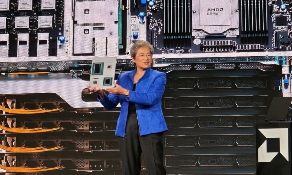
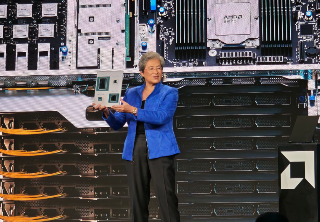
On July 23, at the annual Advancing AI Conference, AMD officially unveiled its sixth-generation EPYC 9006 series server CPUs, namely Zen 6 processors codenamed Venice. The new-generation Instinct MI455X AI accelerator was also showcased. The CPUs are built on TSMC’s 2nm process, while the accelerator combines 2nm compute chiplets with 3nm I/O and cache chiplets.
(Image source: AMD)
The specifications of both chips are incredibly impressive. A more noteworthy shift, however, is that Apple is no longer the first company to deploy TSMC’s cutting-edge manufacturing process.
For more than a decade, Apple has consistently served as TSMC’s exclusive launch partner for its most advanced process nodes. Starting with the A8 built on the 20nm process, followed by the 5nm A14 and 3nm A17 Pro, all these chips debuted inside new iPhones of their respective years. When it comes to the 2nm node, though, AMD beat Apple to the public launch.
Times have truly changed.
Multiple supply chain analysts predict that the iPhone 18 Pro lineup launching this autumn will adopt TSMC’s first-generation 2nm process, N2. Supply chain sources also indicate that Apple has secured substantial production capacity. In other words, Apple still has access to 2nm manufacturing and is by no means neglected by TSMC.
The only difference is that Apple is no longer the first brand to publicly launch commercial products built on 2nm. What’s more, AMD did not debut merely a single 2nm chip this time; it rolled out 2nm products across both its CPU and GPU product lines simultaneously.
The upcoming A16 process paints an even clearer picture. Tailored by TSMC for high-performance computing, the A16 is a 1.6nm-class technology featuring gate-all-around (GAA) nanosheet transistors alongside backside power delivery. Supply chain reports name NVIDIA, rather than Apple, as its launch customer.
Definitive details remain pending, yet the trend is unambiguous. Apple will remain a major buyer of TSMC’s leading-edge processes throughout the AI era, but it will cease acting as the trailblazer driving next-generation chip fabrication for at least the next several years.
Did AMD Claim the 2nm Launch Exclusively Thanks to the AI Boom?
The two flagship chips unveiled by AMD perfectly illustrate why cutting-edge manufacturing has shifted focus from smartphones to data centers.
Take the EPYC 9006 "Venice" for instance. It offers up to 256 CPU cores and 512 threads, supporting 16-channel DDR5 memory, MRDIMM speeds reaching 12800MT/s maximum, and PCIe 6.0 connectivity. AMD positions this chip not only for conventional cloud servers but also for AI host nodes and intelligent agent workloads.

(Image source: AMD)
When most people talk about AI servers, GPUs are the first thing that comes to mind. The catch is that GPUs only handle the most intensive matrix calculations. For an intelligent agent to run properly, additional steps are required: searching corporate knowledge bases, querying databases, calling APIs, running tools, isolating different tasks, and feeding final outputs back to the model.
In short, the GPU acts as a heavy-duty engine, while the CPU orchestrates the entire workflow pipeline.
As the number of intelligent agents rises and concurrency increases, CPU core count, memory bandwidth and input/output capacity grow increasingly critical. By packing 256 cores into a single socket, Venice is engineered to accommodate more workloads within constrained rack space and power limits.
Meanwhile, AMD unveiled further specifications for its next-generation AI accelerator, the Instinct MI455X. This massive chip houses 320 billion transistors, paired with 432GB of HBM4 memory delivering a peak memory bandwidth of 23.3TB/s. AMD will assemble a full rack dubbed Helios by combining 72 MI455X cards, Venice CPUs, Pensando networking chips and ROCm software, designed to compete with NVIDIA’s Vera Rubin NVL72.
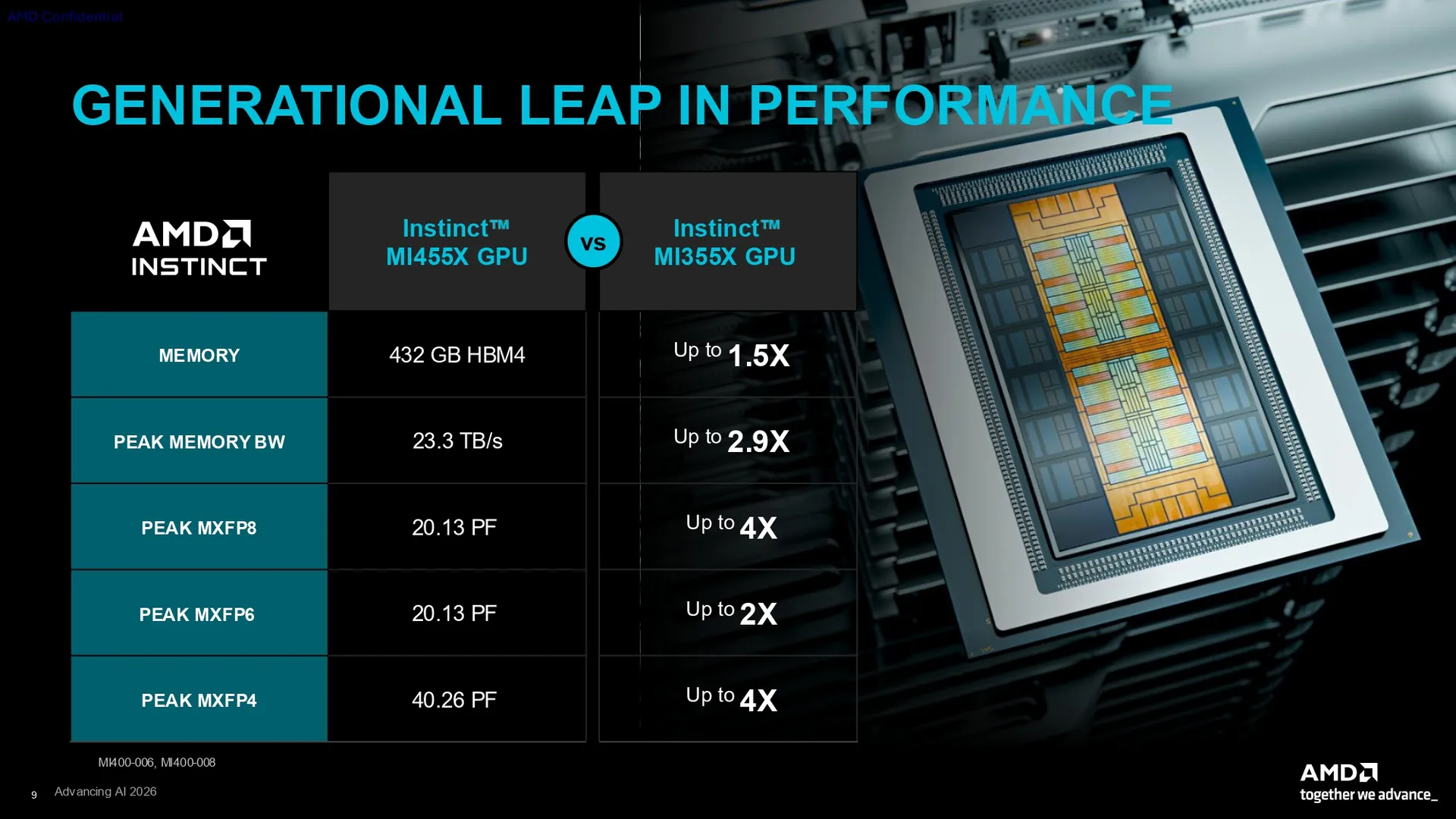
(Image source: AMD)
Additionally, it is necessary to explain how the Instinct MI455X leverages the 2nm process. Strictly speaking, the Instinct MI455X is fabricated with a hybrid combination of TSMC’s 2nm and 3nm processes.
This approach is not unprecedented. Take Intel’s latest-generation SoC codenamed Panther Lake as an example. Its core computing modules adopt Intel’s proprietary 18A process; the GPU graphics modules come in two variants: the entry-level version uses Intel 3, while the high-end variant applies TSMC N3E. Moreover, the platform control unit and basic modules are separately manufactured with Intel’s in-house process and TSMC’s technology.
Cost control lies at the heart of this design philosophy. Similarly, AMD does not insist on manufacturing the entire chip with the priciest advanced process. Following the principle of allocating top-tier resources to critical workloads, the XCD compute chiplets responsible for core calculations utilize state-of-the-art 2nm technology, whereas cache, interconnection and I/O components adopt the 3nm node. These dies are interconnected via 3D hybrid bonding and TSMC’s CoWoS-L packaging technology.
For smartphones, the 2nm process delivers longer battery life and higher peak performance. For AI servers, advanced manufacturing carries more pragmatic value: lower power draw equals lower operating expenses, and higher transistor density translates to greater throughput capacity.
TSMC’s official data indicates that compared with N3E, the N2 process boosts performance by 10% to 15% under identical power consumption, or cuts power usage by 25% to 30% while sustaining equal performance. On a smartphone, this improvement may extend usage time by one or two hours. Deployed across data centers housing tens of thousands of chips, it translates to reduced electricity bills, less heat dissipation demand, smaller server room footprints, and higher token throughput per day within an AI computing cluster.
Of course, the 2nm process is no universal cure-all. Today’s AI chip performance is increasingly governed by HBM memory, chiplet architecture, advanced packaging, high-speed interconnection and software stacks. Even a 2nm chip cannot unlock its full potential if it suffers insufficient data feeding, poor connectivity or flawed software ecosystems.
Nevertheless, with power consumption and heat dissipation emerging as rigid bottlenecks restricting AI infrastructure expansion, efficiency gains have become more valuable than ever before. Consequently, the major buyers of cutting-edge process nodes have shifted from smartphone vendors shipping over one billion handsets annually to large AI enterprises purchasing tens of thousands of GPUs and building billion-dollar data center facilities.
From Competition Between Apple and Huawei to the Race Led by AMD and NVIDIA
Rewind to 2018, when cutting-edge semiconductor processes were dominated by mobile chip developers.
On August 31 of that year, Huawei unveiled the Kirin 980 at the IFA trade show, billing it as the world’s first commercial mobile SoC built on TSMC’s 7nm process. Less than two weeks later, Apple announced the A12 Bionic also fabricated on 7nm, alongside the iPhone XS, iPhone XS Max and iPhone XR equipped with this chip.
Huawei claimed the upper hand by debuting the chip earlier, yet Apple rolled out the A12-powered iPhone XS in September ahead of Huawei’s Mate 20 lineup.
(Image source: Apple)
Both companies could cite their own arguments to claim being the pioneer back then. More importantly, this seemingly nitpicky race for the first launch was essentially internal competition within the smartphone industry.
From the iPhone 6 lineup powered by the A8 chip to the iPhone 15 Pro series equipped with the A17 Pro, smartphones have been the world’s largest, fastest-updating consumer electronics segment over the past decade, and consumers have long been willing to pay premiums for better performance and power efficiency. Flagship phones are refreshed annually with shipments ranging from tens of millions to over 100 million units per generation. This massive volume helps TSMC amortize the enormous capital investment required for new fabrication lines. It also allows Apple, Qualcomm and MediaTek to package advanced process technology into consumer-friendly selling points.
Users can tangibly experience upgrades brought by faster speeds, lower power draw, improved photography, and more recently, increasingly critical on-device AI.
Today, however, the major buyers of cutting-edge semiconductor processes have shifted. TSMC’s high-performance computing (HPC) business accounted for 66% of its total revenue in Q2 this year, while smartphones made up only 22%. In the same quarter, the newly ramping 2nm process already contributed 3% of total wafer revenue. The nearly threefold gap between HPC and mobile demand speaks louder than any industry analysis.
Accordingly, AMD leverages TSMC’s N2 process for its server CPUs and AI GPUs. Rumors indicate NVIDIA will be the launch customer for TSMC’s A16 process. Intel, which operates its own fabs, deploys its Intel 18A process for both Panther Lake AI PC chips and Clearwater Forest server CPUs. The Intel 18A platform is the first to integrate RibbonFET Gate-All-Around (GAA) transistors and PowerVia backside power delivery, with its core merits including high transistor density, boosted performance and reduced power consumption.
One non-negligible detail remains: the first commercial product built on Intel 18A is Panther Lake, a PC chip rather than a data-center component. Apple will also remain one of the largest customers for TSMC’s N2 process.
Cutting-edge manufacturing has not completely departed consumer electronics, yet the forces dictating production capacity allocation, technology roadmaps and industrial clout have clearly tilted toward AI and high-performance computing. Previously, foundries relied on massive smartphone shipments to mature new process nodes. Nowadays, a single AI data center houses billions of dollars’ worth of chips, with operators consistently raising budgets to cut per-token operational costs.
Leading semiconductor foundries are naturally aligning their R&D priorities with this trend.
Closing Thoughts
Apple losing the bragging rights to launch TSMC’s 2nm process first does not mean Apple’s chips have become outdated, nor does it diminish the iPhone’s importance. What has truly transformed is the driving force pushing semiconductors ever closer to physical limits.
From 7nm to 3nm, end users first encountered state-of-the-art chips inside new smartphones. These chips accelerated app loading, stabilized gaming frame rates, and extended all-day battery life for pocket devices. With 2nm, however, the earliest products will be deployed in unseen data centers, powering next-generation AI training and inference inside server racks consuming dozens or even hundreds of kilowatts of power.
Cutting-edge chips have not grown more distant from everyday life. All the search engines, office suites, coding tools, image software and intelligent agent services people use daily run on these chips. The only difference is that this time, advanced silicon transforms cloud computing first before trickling back down to our handheld devices.
July 31 marks the grand opening of ChinaJoy 2026, themed “Journeying with AI.”
A total of 900 entertainment-related exhibitors—including Tencent, NetEase, Sony, Qualcomm, MaiCong, and QingXian—will jointly present a global feast for the entertainment industry.
How will AI-enhanced hardware brands—including terminals, peripherals, robots, displays, and chips—collaborate cross-industrially with game content creators to deliver novel entertainment experiences?
Led by LeiTech founder and Editor-in-Chief Luo Chao, the LeiTech ChinaJoy 2026 reporting team will soon descend upon Shanghai—stay tuned for comprehensive coverage.