
 雷科技
雷科技




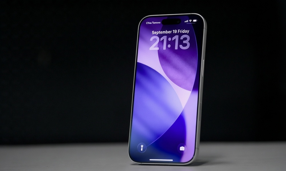

What? Will phone memory overshadow processors?
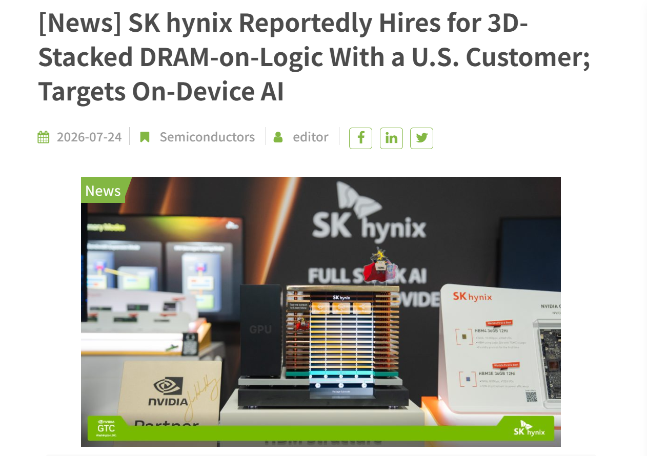
Recently, SK Hynix posted two new job openings in the United States. It aims to tackle performance bottlenecks for on-device AI at the packaging level by researching designs for 3D stacked memory. The company explicitly states it is seeking top-tier professionals capable of close collaboration with US clients. Given the hiring location and past partnership track records, the client in question is likely Apple.
(Image source: trendforce)
Most people will likely be confused upon seeing this news. What does memory design have to do with on-device AI?
Here’s the explanation. While computing power in smartphones has surged rapidly over the past two years, with increasingly impressive figures showcased at launch events, handsets frequently overheat and throttle when running various large model applications locally. Manufacturers are ultimately forced to offload tasks to the cloud, meaning less than one-tenth of AI functions actually run on-device.
This cannot continue. After all, NPUs hyped for three or four years might barely get used before users replace their phones. Manufacturers have therefore set out to identify the root cause. Apple’s finding is that once large models begin continuous generation, performance is usually bottlenecked by memory access. No matter how fast the chip computes, it has to idle if data cannot be delivered in time. That explains why manufacturers are researching 3D stacked memory.
Does more stacking equal faster speeds?
Before diving into 3D stacked memory, we first need to understand how current smartphones are built.
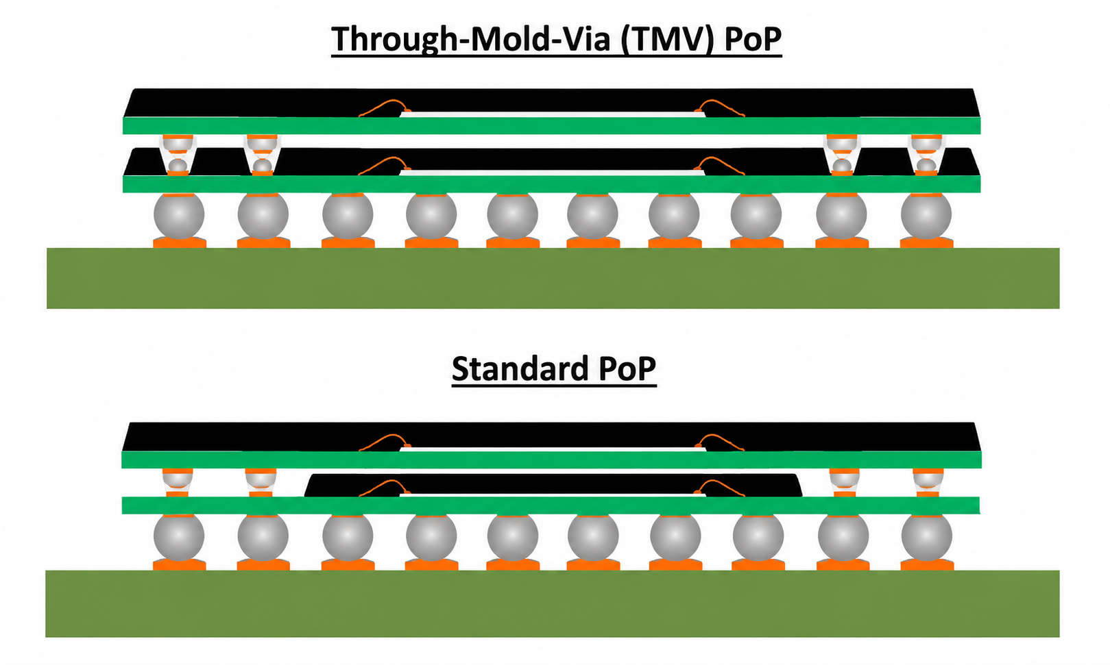
Nearly all mainstream flagship smartphones on the market adopt LPDDR5X memory, which commonly uses PoP (Package-on-Package) stacking packaging: the smartphone processor package sits at the bottom, with a memory package stacked directly on top.
(Image source: LeiTech)
As shown in the image above, although the traditional PoP packaging appears to stack the two components together, a substrate, solder bumps and high-speed interfaces still separate them. Fundamentally, they remain two independent packages. Memory can only transmit data to the processor through a limited number of circuits. Boosting bandwidth mainly relies on raising the operating speed of each channel.
By contrast, SK Hynix’s planned 3D stacked DRAM follows a straightforward concept: remove the outer packaging of the memory, place the bare memory die directly onto the processor, and build numerous vertical data channels between the two chips.
SK Hynix has not disclosed the specific implementation details.
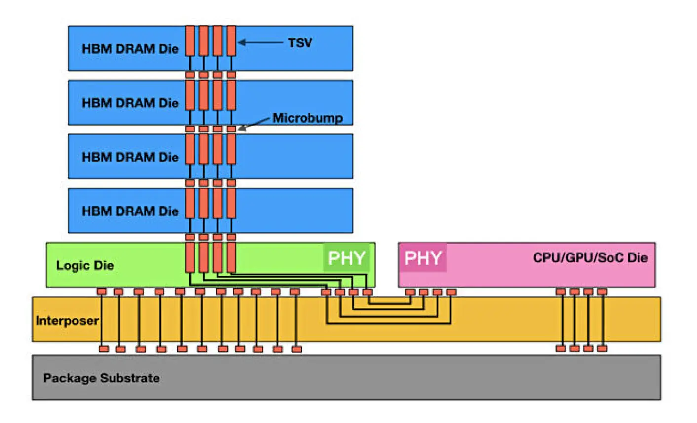
Nevertheless, drawing reference from NVIDIA’s HBM and AMD’s 3D V-Cache, I believe the process will generally involve these key steps: thinning the chips, fabricating vertically penetrating vias inside them, and bonding the two layers directly via copper-to-copper interconnects.
(Image source: AMD)
According to AMD’s official statement, this interconnect approach delivers more than 200 times the density of traditional planar packaging. It effectively boosts the number of I/O ports, meaning the processor can read and write far more data concurrently, while cutting latency, transmission power consumption and physical footprint.
Even if the bandwidth of each individual channel stays fixed, expanding the channel count from dozens or hundreds to thousands or more via 3D stacking can potentially lift memory read/write speeds by tens or even a hundred times.
To illustrate, let us continue with standard LPDDR memory. As outlined above, upgrades for this type mainly rely on raising the speed of each channel. For instance, after Micron pushed the LPDDR5X data rate from 7.5 Gbps to 10.7 Gbps, the aggregate read-and-write bandwidth reached 85.6 GB/s — a tangible improvement over the 76.8 GB/s seen on the current iPhone 17 Pro.
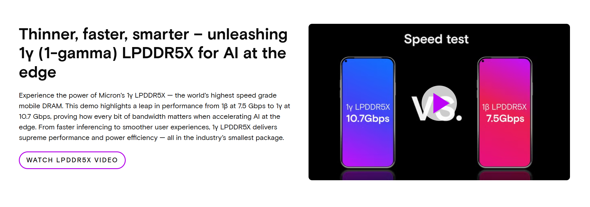
(Image source: Micron)
For comparison, mass-produced HBM4 delivers a bandwidth of 2.8 to 3.3 TB/s.
A technology more aligned with SK Hynix’s concept of "placing memory directly on the processor" is the 3DIMC under verification by d-Matrix. It creates vertical channels across the entire surface of the chip. The manufacturer claims a bandwidth of 20 TB/s per stack with transmission energy consumption of roughly 0.3–0.4 pJ/bit.
That said, the 20 TB/s figure applies to data center chips and cannot be directly replicated in smartphones. What’s more, SK Hynix is still in the recruitment phase, so no one can tell what performance levels it will ultimately achieve.
Even so, the figures disclosed by various players have left me rather optimistic.
Not As Promising As It Sounds
Interestingly, while the smartphone industry is figuring out memory stacking, the PC sector has already experimented with relevant technology.
A couple of years ago, Intel carried out a fairly bold trial with the Core Ultra 200V series. It integrated LPDDR5X memory directly inside the processor package. Though memory was not stacked atop the processor cores, the channel length was drastically shortened compared with that in conventional laptops.
The merits of this solution are straightforward: faster memory speeds and lower latency. Shorter data travel paths naturally cut power draw, bringing an overall power consumption reduction of up to 40%. No dedicated space for memory needs to be reserved on the motherboard, enabling a more compact internal layout. The freed-up room can accommodate larger batteries and enhanced cooling systems.
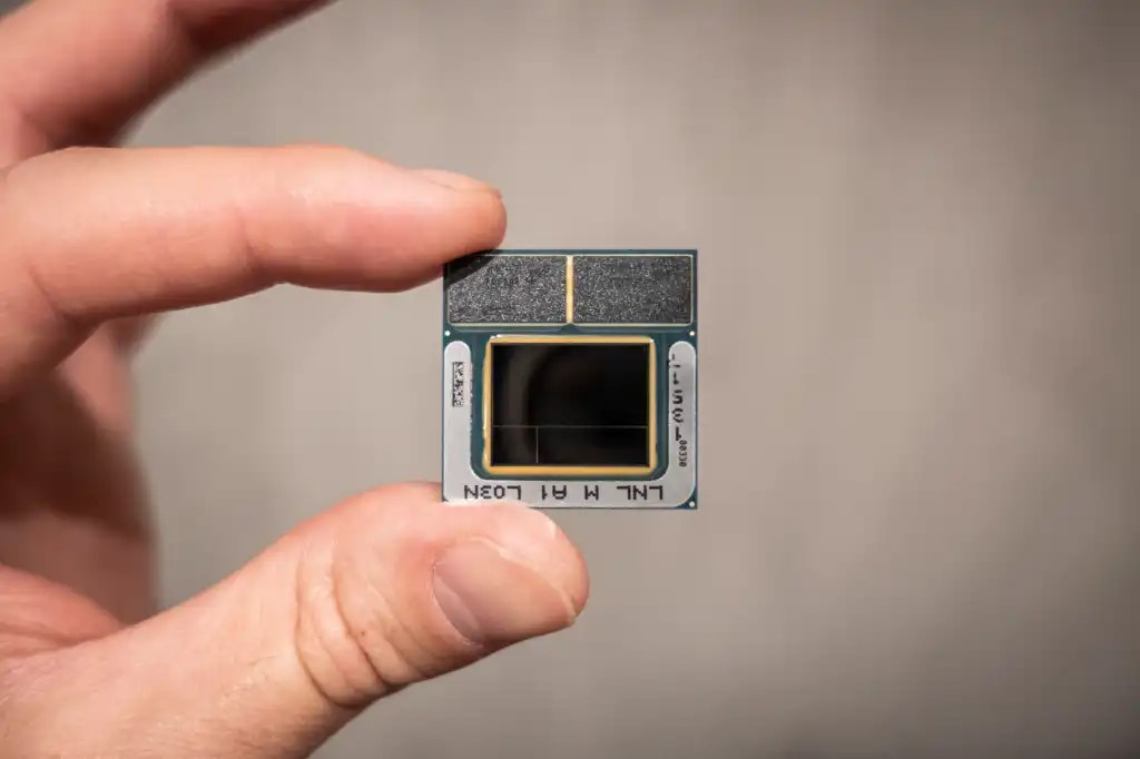
(Image source: Intel)
Crucially, those lightweight laptops delivered solid battery life and integrated graphics performance. This design proved to be a great match for thin-and-light devices. After all, such laptops are never intended for user-upgradable memory. Space savings and lower power consumption make the approach highly appealing by all accounts.
The catch is that manufacturers were unsatisfied.
The Core Ultra 200V series only offered 16GB and 32GB configurations. Once the laptop rolled off the production line, memory capacity was permanently fixed. It was difficult for manufacturers to launch 24GB variants, and scaling up to 64GB was equally cumbersome. Any hardware fault involving either component would incur substantial repair costs.
On top of that, this packaging solution came with a hefty price tag. Most consumers expect thin-and-light laptops to cost roughly 4,000 to 5,000 yuan, yet the Core Ultra 200V series pushed the entry price up to around 8,500 yuan. While these were mostly mid-to-high-end models, they remained out of reach for average buyers.
For the Core 300 series, Intel simply moved memory back outside the processor package. Manufacturers gained full flexibility over memory sizes, ranging from entry-level 12GB single-channel setups all the way up to full 64GB configurations. This greatly simplified supply chain management and device servicing.
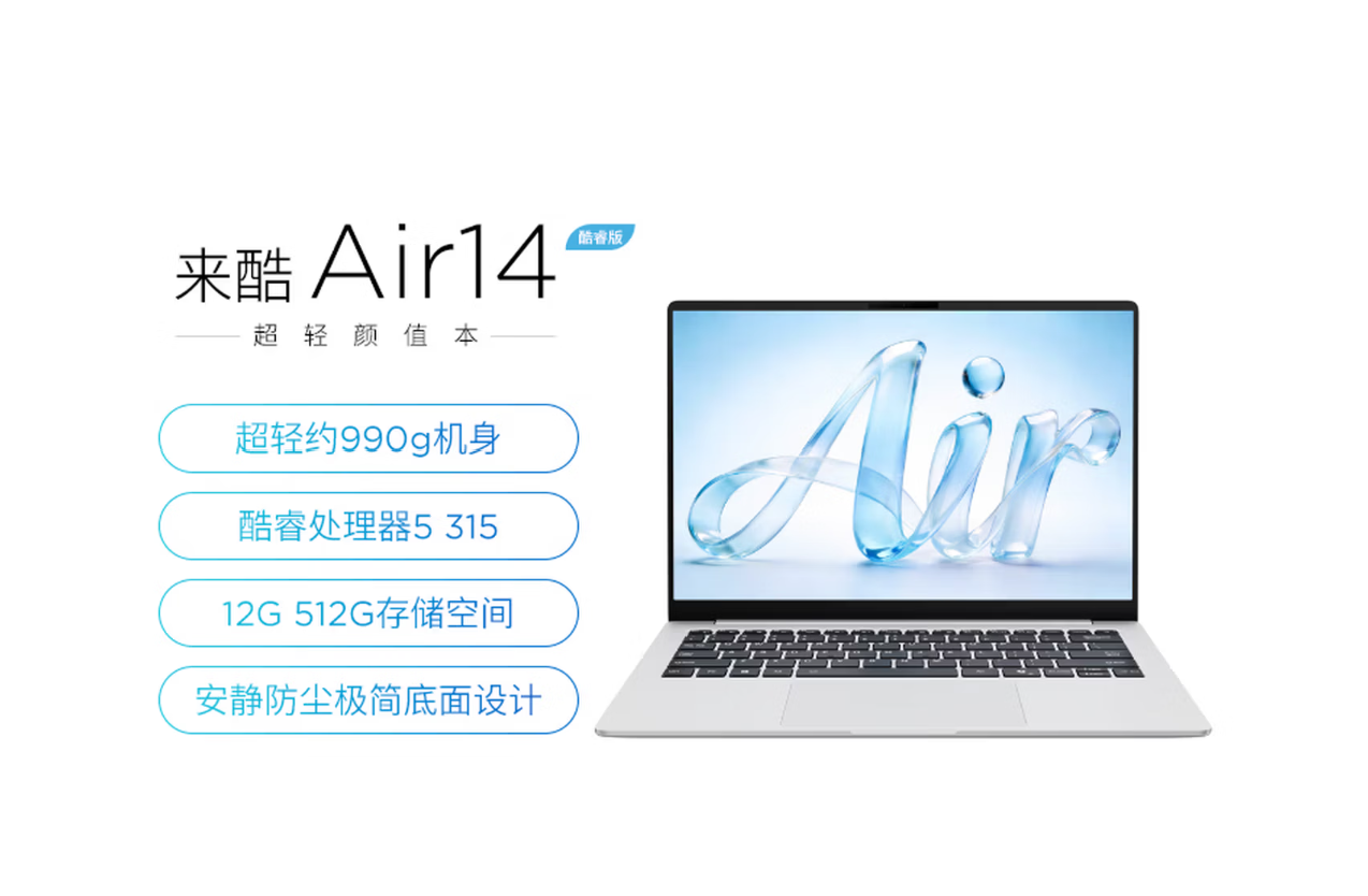
(Image source: Lenovo)
The Xiaoxin Pro 16 GT I have on hand is equipped with the Core Ultra 5 338H and 32GB LPDDR5X memory.
Logically speaking, without integrated packaging, memory performance would inevitably decline, and local AI performance would suffer to some extent. Yet in real-world use, I actually find the Ultra 300 series delivers a better experience than the Ultra 200V generation.
The reason is easy to figure out: the integrated graphics of the Ultra 300 series have seen remarkably noticeable improvements.
The Arc B370 built into the Core Ultra 5 338H boasts a larger scale and stronger performance. Many local large models, image generation tools and voice utilities now leverage the iGPU for computation. Even with a partial loss in memory speed advantages, the upgraded graphics performance makes up for it, yielding an improved experience when running models, processing images and handling other local AI tasks..
In every sense, Intel’s experience can serve as a valuable lesson for smartphone manufacturers.
Turning to AMD, its newly released X3D processors stack extra L3 high-speed cache vertically on top of the CPU cores, adding an extra 64MB of cache per chip. Frequently accessed gaming data can therefore stay close to the processor, drastically reducing repeated memory access operations.
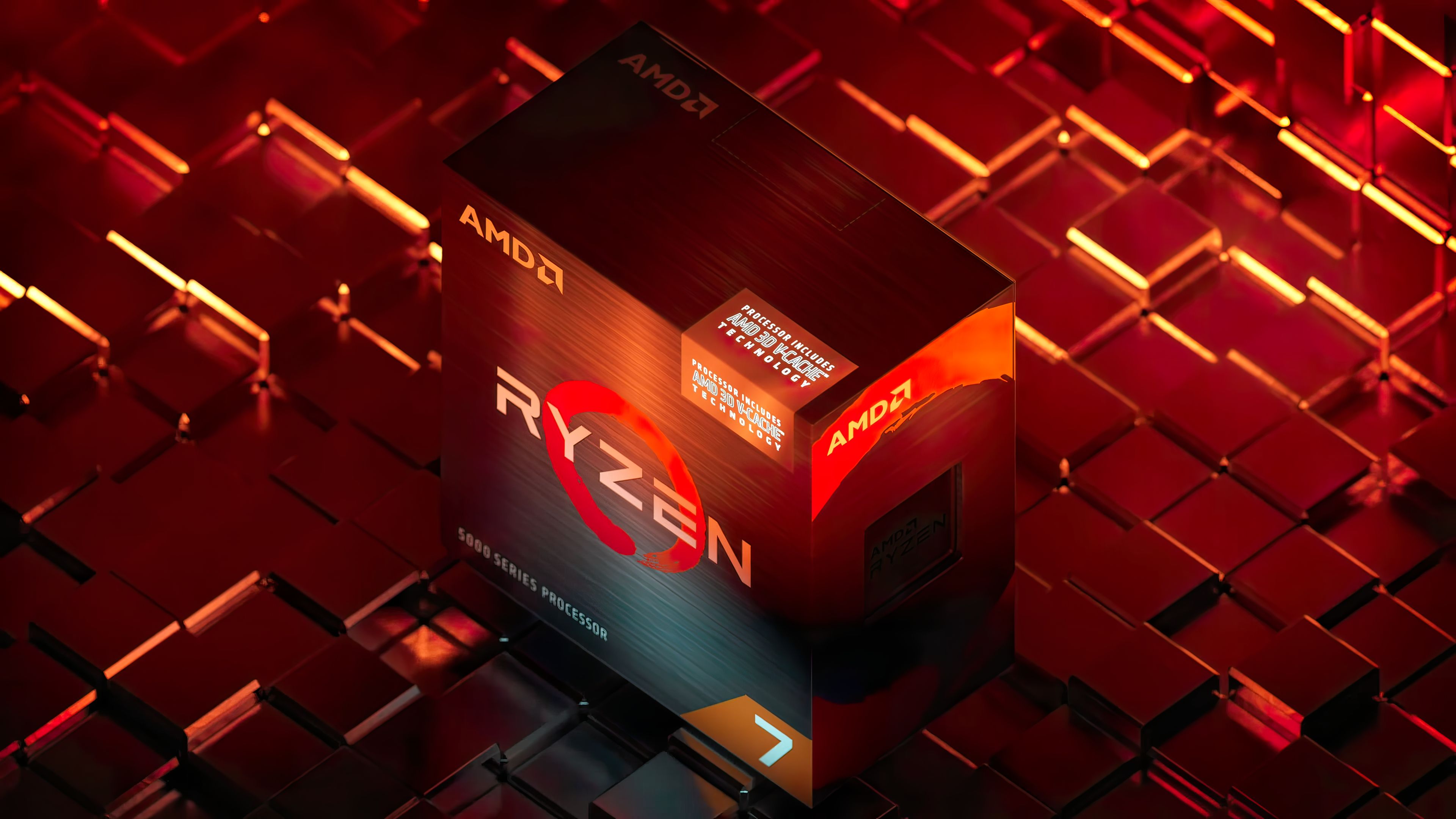
(Image source: AMD)
It has to be said that this approach is remarkably effective. For online games that demand ample cache and low latency, frame rates and stability see substantial improvements. Thanks to X3D technology over the years, AMD has secured a large group of gaming enthusiasts.
However, stacking chips vertically creates a major issue: heat buildup.
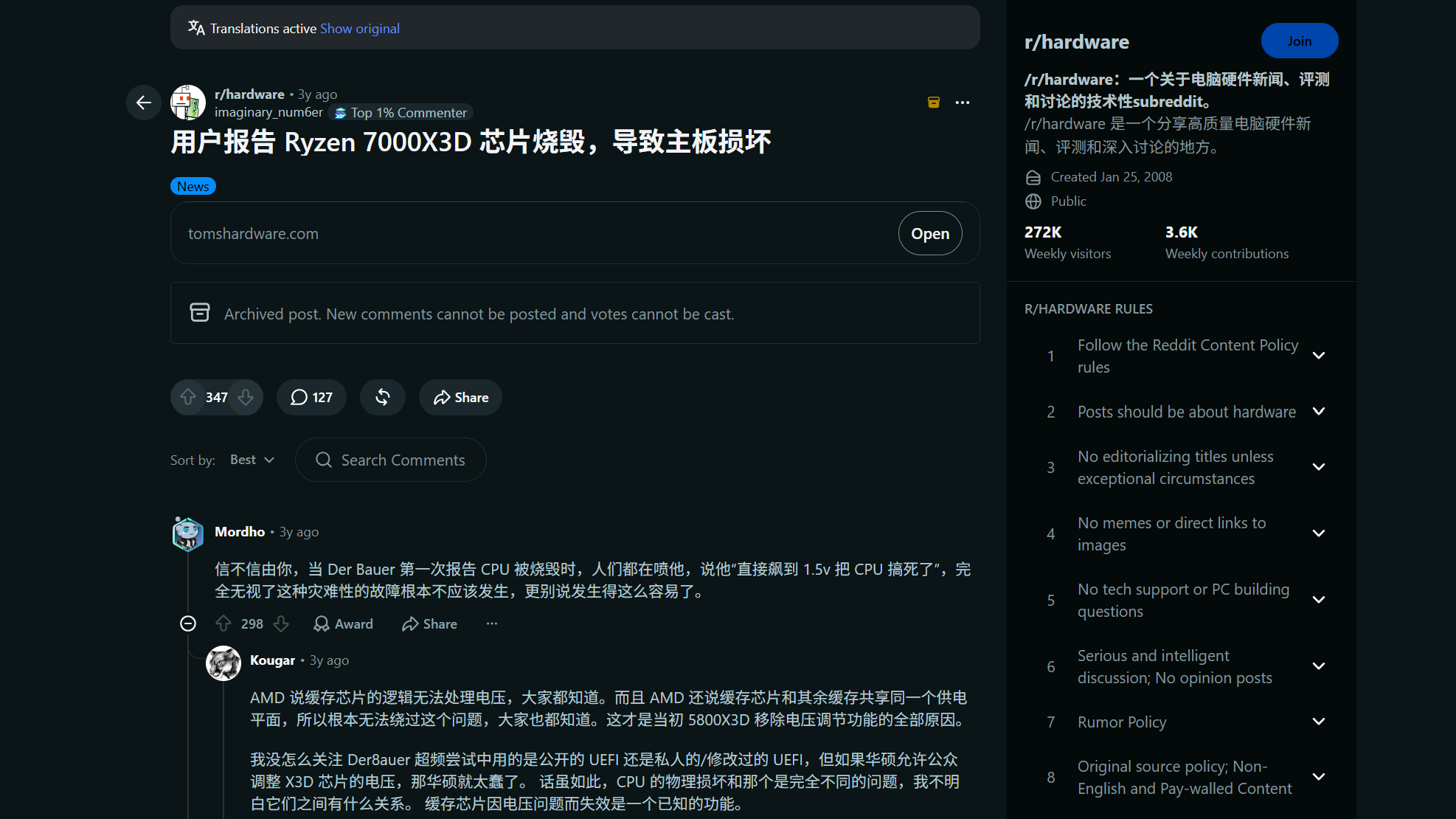
In recent years, numerous users at home and abroad have encountered abnormally high temperatures with X3D processors. In some cases, the malfunctions directly caused damage to other hardware in the PC. The problem spans the Ryzen 5000 X3D lineup all the way to the latest Ryzen 9000 X3D series. For its part, AMD has offered virtually no viable solutions other than working with motherboard manufacturers to cap the SoC voltage below 1.3V.
(Image source: AMD)
Bear in mind that computers come with active cooling. The situation will only worsen when this technology is adopted in smartphones lacking active cooling systems.
Is Stacking the Future of Chips?
From Xiaolei’s perspective, chip stacking will most likely become commonplace going forward.
Now that Moore’s Law is hitting its limits, it is growing harder to boost performance simply by shrinking transistor sizes. Manufacturing separate chip components and reassembling them as needed is an approach already validated by Intel and AMD. SK Hynix is merely pushing forward along this line of thinking.
In fact, the Tao’s Law proposed by Huawei this year follows a similar logic. It aims to break through the physical limitations of traditional planar layouts by optimizing transistor designs, elevate system-level parallelism and efficiency, and cut end-to-end response latency.

(Image source: LeiTech)
Of course, this technology will certainly not make its way into mid-range and entry-level smartphones anytime soon.
High costs, complex packaging, and unresolved thermal challenges mean flagship devices may adopt it as a new selling point to power on-device Agents and local large language models. For phones priced at 2,000 to 3,000 yuan, manufacturers will likely prefer investing resources in batteries, displays and camera systems instead.
As for whether this technology can tackle the bottlenecks of on-device AI, I believe we can maintain cautious optimism.
SK Hynix’s recruitment drive indicates certain manufacturers have begun making improvements at the fundamental hardware level. Meanwhile, companies such as Zhipu AI, StepFun and MiniMax are optimizing large models for edge deployment. Furthermore, Agent applications from several leading brands — Xiaomi Miclaw and Breeno Next — are already undergoing testing. Functionally viable on-device Agents are actually just around the corner.
On July 31, ChinaJoy 2026—under the theme “Journeying with AI”—will officially launch.
A total of 900 entertainment-focused exhibitors—including Tencent, NetEase, Sony, Qualcomm, Maicong, and Qingxian—will jointly present a global feast for the entertainment industry;
How will AI-powered hardware brands—including endpoints, peripherals, robots, displays, and chipmakers—collaborate across industries with game content developers to deliver novel entertainment experiences?
LeiTech’s ChinaJoy 2026 reporting team, led by Founder & Editor-in-Chief Luo Chao, will descend upon Shanghai for comprehensive coverage—stay tuned.